For the D/A conversion, we used an 8-Bit microprocessor compatible, double buffered DAC0830. The DAC0830 is an advanced CMOS 8-bit multiplying DAC designed to interface directly with most of the popular microprocessors. The circuit uses CMOS current switches and control logic to achieve low power consumption and low output leakage current errors. Double buffering allows these DACs to output a voltage corresponding to one digital word while holding the next digital word. The DAC can be used in different modes of operation. We used it in a Voltage Switching Configuration with bipolar output with increased output voltage swing which ranges from -10V to +10V (ie. 0x00 would correspond to -10V and 0xFF to +10V)
There are two important things to keep in mind when using this DAC in the voltage switching mode. The applied reference voltage must be positive since there are internal parasitic diodes from ground to the Iout1 and Iout2 terminals which would turn on if the applied reference went negative. There is also a dependence of conversion linearity and gain error on the voltage difference between Vcc and the voltage applied to the normal current output terminals. To ensure that all 8 switches in the R-2R ladder turn on, it is recommended that the applied reference voltage be kept less than +5Vdc and Vcc be at least 9V more positive than Vref. These restrictions ensure less than 0.1linearity and gain error change. See Figure 3. for the circuit of the D/A conversion unit.
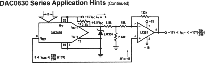
Figure 26: D/A conversion unit.
But we used +/-12V for Vcc and used a 3.3V Zener instead of 2.5V zener, due to lack of availability of the part on time. First we tried out the circuit with a 5V LM336 zener, but the error was so high that the conversion was way off. The error vs reference voltage curve is shown in Figure 4. Since the chip had to output 3 different voltages (to the 3 motors), we needed 3 D/As. So I use port B to output the 8bit digital data which goes to all 3 DACs. But I write to one D/A at one time. So I use 3 pins of port C to control the 3 DACs, making one of the pins low at one time, thus enabling the write for that D/A. This way, I have the chip output data to all the 3 D/As, thus controlling the 3 motors.
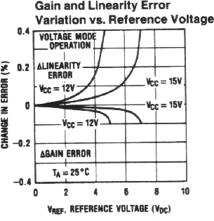
Figure 27: Error vs reference voltage.